
Hello JS
I am so happy that you are getting a board to test out. It sounds as if we are on the edge of getting things resolved as far as heat. From what you said above, I will solder on another set of fets tonight and see where that goes on the scope for starters.
Dana
-
HiOriginally posted by prochiro View Post
it is not necessary to prepare a question like this. We all now there are no silly questions but answers only. So sit back and leave the madness to the person being requested to answer
Answer:
1. Yes it IS possible and state of the art but we need to have a close look in order to not have more FETs switching even worse.
2. The protection circuit was doubled in order to prevent overload of the protection circuit itself. Some few components need to be multiplied if (1).
Unfortunately I was not able to measure and optimize the true PCB circuit up to now. But this will be my absolute priority in next time. My concern will be switch speed, spurious oscillations, protection functions in case of all sorts of overloed. And I will check 4 FETs as well in the end.
In fact you will add two more FETs at other side of PCB connecting D, S leg directly. Each gate needs to have an:
- Individual gate resistor (needs to be tuned).
- Protection diodes at gate
Fortunately I have now the equipment for thorough measurements. (Our lab was reviewed and I could get some valuable devices for free).
Hint: Please understand that we deal here with much more facts than switching current. For normal understanding those facts are covered (quite similar to free energy basics). For short timeslots we deal with giant current increase per ns along inductivities in nH range along high frequency well above several 100Mhz. Those are the building stones adding to nice and rugged switching actions. The conditions are similar like entering in microscopic realms.
@Cornboy: YEAH! That is the way to go. You step back and check the driver. Thus you learn deeply getting an x-ray view to circuits later on.
Those Micrel drivers are designed for rise 20ns / fall 24ns into 15nF gate capacity. You see they do not give unrealistic data without load but with true realistic load added (15nF). Therefore you have those 12ns (without load) - better than data sheet.
Our FETs have about 6.5nF at each gate. (In fact it is a bit worse at true load conditions but let start here) You observe that two FETs are well aligned to Micrel data sheet (13nF vs. 15nF)
For education you may want to test:- Observe and note: rise AND fall time in unloaded conditions.
- Adding about 15 nF load to driver output observing signal like above. Add caps short leaded. (Not exact values required. 22nF will be OK as well or you add several 4.7nF or 4.3nF caps in parallel)
- Adding another 15nF (about 30nF total) in order to check for 4 FETs (that is related to Dana's question)
- Leave load like above: Adding another couple ceramic caps to power leads of Micrel driver in order to check if slopes getting better or not. If better: blocking with caps needs to be reviewed. Remember this driver is able to shoot up to 12A into the gates for short time (below 30ns total). There is no chance to get this amperage out of PSU via long leads. The sole source for this batch of electrons are those ceramic caps at power pins of FET driver. Those caps are somehow a coulomb stock for very very instant retrieve - prioritized like top emergency cases in health business.
Posting your results will be a superiour education for you and the whole community.
PS: Ah, just got it: You were able to operate that zoom function - great
JSLast edited by JohnStone; 09-11-2013, 02:32 PM.Leave a comment:
-
Driver section.
Hello All, i had a little time to get back to Monster, so i decided to start from driver section, disconected, gate resistors so no fets in the equation.
Just wanted to see voltage and steepness of edges. It appears to be a good square wave, and streched out to 5 ns/ div takes 12Ns to rise, and is over 12v. God it's good to have a scope, even if i can't use it properly yet.
Does that look all good everyone?. If so i will connect the gates directly first and check, no load and then resistive load, if a problem with ocillation occurs, i will go up on resistor values and see.
Will keep you posted with pics.
Regards Cornboy.
[IMG] [/IMG]
[IMG] [/IMG]
Leave a comment:
-
Strange Question
Hello JohnStone
There is this hypothetical person who has a hypothetical question. The question is; if he was stupid
  enough to make one monster driver with four fet's,
 would he need to put the complete set of diodes and such for protection on each fet or could he just put one set of protection on each side of that single board? I told that person what you said but he is hard headed and wants to try it. What do you say.
DanaLeave a comment:
-
I checked my last layout and the one you got from Oshpark. It is the very same circuit except some minor adjustments. Those two jumpers are the one major modification. I sugeest to continue using thisl layout in order to prevent any further confusion.
Let's test this layout to the very end. Thanks Cornboy for your spare board. I'm eager to assemble and test it.
In case my tests suggest some mods we will get another layout double sided and shrinked in size.
BTW: Oshpark did not aswer my mail to "[email protected]". Is there another mail address at oshpark available?
JSLast edited by JohnStone; 09-10-2013, 08:09 PM.Leave a comment:
-
Kogs
That dropbox address is your home computer address for the file.
DanaLeave a comment:
-
Hi Kogs,Originally posted by iankoglin View Post
those 78xx voltage regulators are specified 10% or 5% accuracy for output voltge - depending on type. They need approx. 2V higher input voltage than specified output voltage.
Additionally you should check your meter. It might add additional tolerance to the measurement. Jamming all tolerances together gives your voltage figures.
Anyway the regulators seem to do well. Last check will be loading them with 100 ...300 mA load (bulb or resistor) each and recheck input voltage and output voltage. Remember to have at all conditions minimum 2V higher voltage at input.
JSLeave a comment:
-
G'day Sampojo, John Stone and teamOriginally posted by sampojo View Post
@ Sampojo
By moving the Opto up a bit then there was enough room to let the lands go between the legs of the Opto rather than having to add the 2 Jumpers.
Also when making the inquiry ask if they can double up on the circuit with another layer a copy of the first in that way it is like adding extra solder but there again Dana said his runs much better with the extra solder he placed just like John Stone said in the first place we need to make the connections by building up the lands with heaps of solder,
@ John Stone
Thanks for your tutorial it's really helps to understand how you have designed this monster so we can Debug it later if need be
I am now loading a new Monster PCB that I have etched using "PCB in a Box"
I have loaded and tested the first 2 sections first the 12v and then the 5v.
I loaded and then Tested the 12v using a 36v (3 - 12v in series) through an adjustable Regulator 40vin adjustable by a trim pot down it has a LCD viewing switchable to Vin and Vout I connected this up through the PCB connections like you said I can then regulate the Vin.
I then connected another same as above only this one I used only to read the output of the 7812.
I started with Vin@12v and adjusted up until I could read the output of the 7812 would reach 12v the maximum I could reach was 11.8v the Vin was 14.8v and if I went any higher it would still only read 11.8v so I left it there.
Next I connected the 7805 circuit and leaving the PCB Vin @14.8v I checked the Vout of the 7805 and it was 4.8v
I imagine that perhaps the adjustable regulators I have are not correct and so I have left them and will continue on tomorrow with the next section.
Kindest Regards

Kogs still here no thinking allowed so I do it quietlyLeave a comment:
-
Monster Driver V5.1 Jumper Question Info Collected
Pulling all this together trying to make it easy as possible for all buyers of the MD V5.1
Originally posted by Cornboy 555 View PostDiagram shows jumpers circled in RED.Originally posted by iankoglin View Post
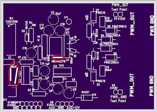
When I first noticed these three lines on the board I immediately suspected they would be jumpers. However, I checked the isolated one near the the opto IC, and found it to be like the jumper was already in place, a completely closed circuit at its 2 endpoints. (Hmm, so I guess if they are jumpers they are already in place?) (NOT!). So I didn't bother to check the other two, assuming they would be the same. However they are not as Cornboy has been finding out. So this difference does make you wonder why, but so far nothing serious.
So I will examine these new files, prep them for OSHPark, send them over and see what Laen (Jim Neal at OP) says, but first I will give John Stone some time on what should we do about any versioning. Such a minor thing maybe we could just slip in the improvement without the change, but I am still confused why the opto jumper is already wired by a PCB trace. Again, very minor.Leave a comment:
-
On it's Way.
Hello John Stone, black monster is in the post to you, they said 3 to 7 days, it will be interesting to see how long it takes.
Warm Regards Friend, Cornboy.
Leave a comment:
-
G'day SampojoOriginally posted by sampojo View Post
Here is the link to the latest version of JS's Monster driver where the Opto isolator was moved and the lands going under the Opto chip rather than having 2 Jumpers
https://www.dropbox.com/home/John%20Stone
Kindest regards
Kogs working in the backgroundLeave a comment:
-
buggy code
@hitby13kw and all
That code was buggy so I pulled it after debugging and decided to issue the new version. version 0.0.5 is the same as version 0.0.3 except that it has been debugged and version 0.0.6 is the same as version 0.0.4 except debugged. There were enough problems that I felt issuing a new version would clear up any problems with the older versions. But your efforts are not in vain as all versions are built upon existing versions and the tutorials are built from previous tutorials with added features explained in the newer tutorials. Good luck with your efforts. Let me know if you have any problems with these versions.
Cheers
GarryLeave a comment:
-
Monster PCB
If FETs heat up at relatively low load they suffer on bad or unsolicited repetetive switching - usually. Of course bad switching comes along bad signal edges and therefore SHE will disguise.
Any oscillation or other distubance at gate can cause semi open DS junction => heat. Forbidden range is about 3.5V ....9.5V. This range shall be crossed as fast as possible. Even flashback from heavy oscillations at source pin shall not enter this forbidden area at gate pin.
1. Till suffering on order / delivery implications from Oshpark. I'd like to test exactly that make of PCB you suffer on. But there is a silver line at horizon - Cornboy is so kind to supply his spare board to me. I will populate and measure ASAP.
2. Regarding jumpers and version: Need to investigate - will reply soon.
JohnLeave a comment:


Leave a comment: