If this is your first visit, be sure to
check out the FAQ by clicking the
link above. You may have to register
before you can post: click the register link above to proceed. To start viewing messages,
select the forum that you want to visit from the selection below.
@ All
I have a few pictures below of the way I plan to do the input/output from the two fets in JohnStones Monster PWM. I have the triangle small and equal with battery cable ends hammered flat and cut short to solder onto the leg of each fet. There are two sets, one for source and one for collector. They fit one inside another with strong clearance. They will be bolted directly to the (#2 gauge and short as possible) leads.
Dana
Yes Dana that's great! But please be careful if you solder those sticks to FETs in order to not kill them by heat. That is: presolder the FET legs, preheat the wire terminals with much heat, attatch the FET legs and solder FAST, cool down fast with pliers or with some kind of spray (inert) or simply with wet sponge. You might need a third hand for help.
JohnS.
....
But I think that for your project I recommends Arduino Mega 2560, it has 54 I/O pins and newer USB comm like Leonardo.
One important feature is that Mega has 4 16-bit PWM Timers so I think it will help when we make your 6 stage PWM.
....
Hi Nico,
I agree with you totally - from technical view. But it might be essential that all of us use the very same processor platform (i.e. 328). There is no other way in order to provide newbies like Cornboy and many others unnamed with programs being fully shareable.
Newer platforms differ in USB to be native in order to enable USB native protocols in order to simulate keyboard, mouse to a PC. But this is of no concern for us.
Another concern is the basic form factor:
1. Native form factor requries a "shield" fitting to the connectors of arduino istself.
Native Arduino form factor:
Arduino shield for additional electronics:
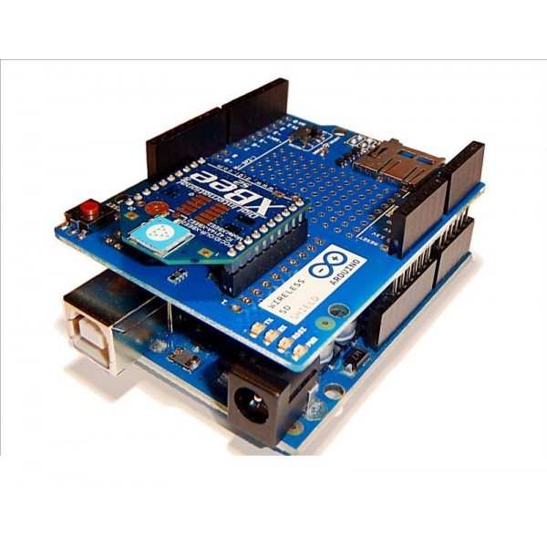
Ardunio stacked with sield:
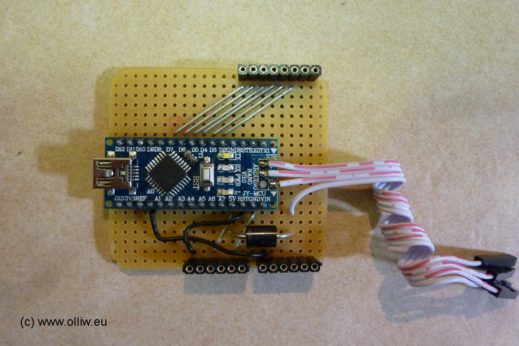
2. Slim line: nano, Tosduino ... can be mounted an a normal IC socket at our breadboards.
Prepared for DIL socket:
Example:
Usage:
It can be made ready for screw terminals s well:
Now my question is: what formfactor and processor type will help our community most in order to get various electronic tastks done easy? We are loaded with the task to recommend a unified solution because most contributors can not decide themselves. And they are not able to modify given solutions to their specila setup.
You Nico and I are fans of the small form factor #2 becaue of very easy adaption ot bread boards. Others might go another way.
We shall decide at least for ame procesor pltaform. Different formfactors might be dandable.
Nico, please understand, I do not want to argue but get for our untrained members most of eficiency.
BTW: For Cornboy it might be more easy to pulse 2 or 3 channels by one arduino and get them synchronized by another master Arduino. Else it would be very difficult to help him in case of problems. Any problem case needs to be devidable in componentes in order to debug them separately.
I am using Arduino Nano, it is similar to Arduino UNO but smaller and can be mounted directly to a breadboard.
Leonardo: is a newer version, it has more I/O pins and better USB comm.
Micro: Is Leonardo but smaller, like Nano.
But I think that for your project I recommends Arduino Mega 2560, it has 54 I/O pins and newer USB comm like Leonardo.
One important feature is that Mega has 4 16-bit PWM Timers so I think it will help when we make your 6 stage PWM.
I am not an expert in Arduino but wish I helped you
Hello John Stone, Nico, Dana, and all,
A question please if you wouldn't mind, not taking cost into account, which Arduino would be best to pulse 6 different channels at once, and give the adjustability UFO talks of.
At this stage this technology is completely new to me and may need some help.
@ All
I have a few pictures below of the way I plan to do the input/output from the two fets in JohnStones Monster PWM. I have the triangle small and equal with battery cable ends hammered flat and cut short to solder onto the leg of each fet. There are two sets, one for source and one for collector. They fit one inside another with strong clearance. They will be bolted directly to the (#2 gauge and short as possible) leads.
Dana
@JohnStone
I understand the triangle design and that is cool. What I was asking about is the size of wire to use for the triangle. On the drawing it states (thick insulated). Should thick wire be 2 gauge as per 100 amp. charts or can it be maybe 6 gauge without any slowdown for that short distance? Whatever size of wire I will make from many strands into one large triangle shape and insulate it as one wire. The word thick may mean different to different people.
Sorry for confusion.
Dana
Ah! My error! OK: There is no general answer because it depends strongly on application. But let's try an approach:
You need to decide what losses you accept.
Given you have 1m of wire and you accept 1V loss between battery and destination point. Sounds like viable!
1Ohm @ 1V will ocuure at 1A
0.1 Ohm @ 1V will occure at 10A
0.01 Ohm (10mOhm) @ 1V will occure at 100A
If you look into the AWG chart you will find a correspondance for 0.010OHM (=10mOhm) / 1m to be AWG15.
Now let's calculate losses:
1V times 100A = 100W! It is a nogo! So we decide that we will not accept 1V loss of voltage.
Search in the AWG table for 1mOhm -> AWG5.
Now you have 0.1V voltge loss and 10W power loss. Your wire will get quite warm and might overheat.
Let's reduces power loss again to 5W per m ...
You search for 0.5 mOhm and find AWG2. -> 0.05V / 5W power loss.
Now we understand the wire diameter provided at those battery clamps!
AWG2 corresponds to a wire with diameter of 6.5mm / 1/4"
Summary for wire 1m @100A:
AWG15.....1.000V loss........100W per m
AWG 5......0.100V loss.........10W per m
AWG 2......0.050V loss .........5W per m
Once again we find: Blessed are those people using short wires!
If you decide to use 20cm of wire you have losses of 10mV / 1W. that's fine.
JohnS
@JohnStone
I understand the triangle design and that is cool. What I was asking about is the size of wire to use for the triangle. On the drawing it states (thick insulated). Should thick wire be 2 gauge as per 100 amp. charts or can it be maybe 6 gauge without any slowdown for that short distance? Whatever size of wire I will make from many strands into one large triangle shape and insulate it as one wire. The word thick may mean different to different people.
Sorry for confusion.
Dana
Got it.
I was able to copy and make a part for the MIC4452.
The other one's did not show up in any parts library I could find for
Eagle. I did not want to spend to much time looking if I could learn
how to make one quickly.
I have the schematic done, now I need to place the components on
the board. I will lay it out as close to your board as I can. The schematic
looks almost identical to your program as well. The board will be 80mm x 100mm.
I dont need to use the whole board but that is the size I have set up on the
CNC. I can do double sided boards without alignment issues.
A few questions.
Resistors R9 and R3 (optional tuning) you have them as regular resitors.
IF these are there for a future upgrade, do we need more room for them?
Test points K2 & K3 pins 1 and 2 are connected? (Just want to be clear)
And last the V-Gen point (pin 6) are these going to (74HC132n) IC4a pin 3 and
IC4b pin 6? When drawn this way in Eagle it does not like it, but as long as
I have the traces right, I can over ride it.
Mark
Hi Mark,
thanks or contribution! Regarding R9/R3: Those resistors are of the smaller type 204 and not normal 207. If you layout that part use SMD resistors 0805 or smaller. It is not the wire length itself to be short as wires have an approximate propagation delay of 1 ns for every 6 inches (15 cm) of length. They gather underway inductance and resistance. Epecially the inductance forms along gate capacitance resonant sicuits. Those can oscillate far faster than switching time posted in data sheet. You possibly can ot see them at your scope but they derate the setup. In this case we introduce those resistors for sanity of switching. But they derate the current flow and thus the switching speed gets considerably slower. Normally 1 Ohm is too low to stop oscillations. On teh other hands those resistors need to pass 12A for short time. This is a major delemma. But if we have SHORT wires and proper layouted cap, driver gate, source and return we might omit any additional resistor - thus optimal conditions.
Regarding test points. Yes connected in order to enable connection of several leads. Regarding V-Gen point (pin 6): K1 pin 6 is a resting point only if you somehow need to deal with teh V+ from generator. It is not connected at all , nor to any output off the gates. Seems to be a kind of transfer problem.
Regarding gate IC4A and IC 4B: If you conenct one input pin only to GND it will suffice. I had no GND around at my layout and needed to connect both to + in order to get them quiet.
Start layout with driver and FETs. Make it symmetrical and short and less bends. Provide a GND path from source pin back to driver in parallel or above/below drive path from driver to gate.
Continue with protective parts and consider 650V from drain along protective elements (= povide copper free areas in order to protect from sparking)
Add copper planes on top and bottom in the FET areas if possible. You might send this part for review first. Al the rest is not critical aexcept proer GND connection. My program does not allow to draw different GND grades.
BTW: The protective diodes need to be adapted to FETs. I chose these for Infineon 650V. I choose two in series in order to minimize capacitance to gate. Imagine the FET being switched off and a spike of 600V. Any capacitance will transfer this voltage rise to gate and try to reopen it. One unidirectional diode adds 600pF in this area. A double sided 150pF, two double sided 150pF..
All those components around the FET can be obtained in SMD. This would give a superiour setup. But this is your very personal decision.
Here is a pdf. of the schematic done in Eagle.
Please let John S. approve this copy, and use his schematic
for building your boards. DONT use this for layout of building
your boards. This is only for those who will use a CNC to mill or
for eching copper.
Mark
CA = bidirectional side.
P6KE15 should be P6KE15A = unidirectional (I need to correct ist as well.)
Ther rest is super! Thanks
Layout:
Consider the GND system right hand from driver to be differnt from GND system left of driver. Provide only on thick and short wire from IC5 pin5 and Ic5 pin 4. Study data sheet of MIC4452. Same at pin1 and 8
Connect GND from IC5 pin 5 direct to sources of FETs and while running in prallel or below / above the gate drive from pin7,8 to gates. Connect all circuitry around FETS directly to respective source pins.
Thus the source pins are th only GND hub between driver and FET circuitry.
If you know all these matters please ask me to not repeat them.
............................
On the 100 Amp line from fets to board pad, we know that large wire is needed but should we try to get 2 gauge as per 100A requirement or do you think something smaller would suffice? Although 2 could be done, do we need to go that far at least to the pad? What are your feelings about this. I suppose the same question would apply to the power input and output as well. I see that whatever it is, will be mounted on the top and be a bolt thru on the pads. I wonder if a small copper bus for the pads, at least on one side might be better or not. The last part I need will not be here until thursday.
Thankfully
Dana
Hi Dana,
can't decode exactly what your concern is. The reason for this hand wiring is to get both FETs on very same duty. Thus I suggest to connect sources and drains first. Stranded wires preferred or massive Bus bar out of copper.
If you use 1,2,3 wires in prallel does not matter.
The next concern is to tap this bus bar in a way in order to pertain SAME duty. Either you build a triangle like I suggestd or you tap the bus bar exactly in the center between both FETs.
Look at PC PSUs how they connect a plurality of wires to one single conenction point. In our case it will be an advantage to crimp all wires to one crimp point (like automotive crimp technology)
and solder this crimp ring to the pins of the FET.
Example for bus bar. Those are for 80A 100% duty.
Hope it clears your concerns - else ASK!
JohnS
All of you who do not know the other tread of Ufo be announced that I released the monster pulser V5.1. 100A 600V
You find relating data here.
It can be built on a bread board type "pad per pin".Discussions shall be performed in this thread. No ready mad PCB required.
JohnS
Hi friends,
as Machine lost his FETs recently I want to show you how to get a FET stage into operation while having your FETs and meters safe.
As we humans are not able to comprehend a fault instantly and precisesly we need to slice the problem BEFORE we suffer on it. The proved method is proceeding step y step. And please note: In most cases the problem sits there and stares with its eyes onto the circuitboard Be aware to be erroneous!
Hint: You will be asked later on to connect a overvoltage protection and a peak voltage detector. You will find those elements in the circuit diagram below.
1. Action: Do not use coils in the very first switch on but a resistor or car lamp or similar ohmic load. Calculate the max. current at permanently switched on stat to not be grater than 80 % of the max. current out of data sheet. Mount your FETs on a heatsink. Check: At every test check temperature.
2. Action: Attatch the overvoltage protection to FETs
3. Action: Start with 12V first.
4. Action: Operate the FET stage manually first - disconnect from generator. Thus you can measure with simple DVM and thoroughly.
5. Action: Connect input lead to GND.
Check: Measure if your FETs have less than 1 V on gate. Light at output OFF! If not: measure where the the voltage originates.
6. Action: Connect input lead to 12V
Check: Measure if FETs have 10V minimum at gate. Light at output ON! If not: search for the loss of voltage.
7. Action: Connect generator with low frequency ca. 1Hz
Check: Watch function: on / off / on ......
8. Action: Add in series to bulb at output a coil. Replace the output load by a moderate coil. Attach a neon (overvoltage protection) across SD of the FET.
9. Action: Operate generator faster i.e. 100Hz. Connect a home brew peak detector, connect DVM. Check: If neon lights at this step you have too big coil or too low frequency.
Wait DVM reading being stable. Now you have the exact peak voltge less 0.6V beacuse of the diode. Action: Discharge the cap from peak detector after every check.
10. Action: Remove the bulb at output. and connect coil between Battery and FET directly. Repeat #9.
11. Action: Increase battery voltage or use bigger coil (or motor).
Repeat #8 Check. Neon on? procede with #12. If you have now not your final load increse load step by step until neon gets on dimmly.
12. Action: Neon is now on dimmly while FET stage running. Note the peak voltage.
13. Action: Check the data sheet for max. voltage DS. Take 80% of this voltage and devide it by the neon voltage + 1V noted before. The integer number is the number of SAME neons you can connect in series between DS of FET in order to get a reliable protection from overvoltage. Check. Neons shall not light up at all while normal operation. Measure the peak voltage to be below 80% of FET voltage and note the voltage red.
14. Action: Discionnect overvoltge protection (cap/resistor) Check: Recheck like #13.
15: Increase freqeuncy step by step.
Check: Temperature, neons to be off, voltge at peak detector....
Hint:
- When operating assymetric motors high voltage spikes are intended. Therefore neones shall light for exceptional protection only. If the lihgt up you should replace FETs by higher rated components. Calculate the cont of neons again (#13)
- Recheck overvoltage protection if you make your FETs switch faster as well. The calculation for voltage spikes depends on switching speed as well. They are build up by load voltge, amps being switched off and switching speed.
Small 12V motors can develop spikes up to 150V and more. An ignition coil being fed with 12V / 3A will produce up to 300V spikes.
- Your setup will not be protected while you read this text. YOU MUST DO IT YOURSELF!
Here is the new coil i built to the specs given earlier. The magnet only levitates at a specific duty cycle and frequency. The transistors are MJL21194. I tried FETs at first but they put out so much power they blow out the light bulb loads and then blow themselves out and sound like fire crackers. Especially on 36V. My signal generator only goes up to 1.8 kc so i may be able to get more power out of the coil if the sig gen will go higher. I just wish there was some sort of safety device so that if the loads blow out , the fets or transistors would still survive.
If you run my two tutorials above plese adjust the slider for current speed. Depending on your computer it might run too fast or too small. Adjust it so you can wathc the balls runnign and have an imagination of the direction they fly.
Sorry for that I realized some minutes later and corrected it. please try it again now.
EDITING: Please press the button "advanced editing" additionally after "edit". That area edits quite well!
You asked regarding importance of delay time at FETs:
If you calculate a cycle of switch on and off you have to add:
on delay i.e. 130ns
switching speed i.e. 10ons
off delay i.e 103ns
-----------------------
summed up: 333ns
The FET is able to switch within this time on and off (330ns) completely but there is no flat part on top - just a cone shape only. The period of 330ns corresponds to 3MHz. If we want to have nice square shape we need to take the period 10 times (3300ns / 300KHz).
Now comprehend the notions above as performance at ideal conditions. In reality we possibly need to add further deratings due to poor driving, heat .....
Let's calculate real 200KHz to work fine.
This will be more than siffitient for UFO circuits - given you operate at 50% duty cycle. If you decide to adjust 10% (factor 5 copmpared to 50%) duty cycle the shape of a songle pulse behaves like 200kHz times 5 = 1MHz. Thus the pulse will not be of nice square shape. 10% duty cycle will be fine at 40 KHz only.
The elaboration above relates to having nice quare shaped pulses on the scope, avoiding unwanted side effects and heat problems - quite normal and sane procedure for basic setup. But there is more to it.
Very independently from nice squares SHE does not care of pulse shape but on steepness of the edges only. SHE forwards a flash of energy at every switch off edge. The energy of a single flash will increase with the steepness of the edges. This is essential! Every edge adds another chunk of energy. AH, the frequency is an effect as well! Yes well, but it is much more effective to get fewer but strong flashes than many and halfhearted ones.
And please note that steep edges when pulsing a coil generates HIGH spikes at FET.
I hope to have explained on why I prefer fast high voltage pulsers. Ufortunately RDSon, Voltage DS and max. amps affect each other and we can not have all at same time. Fortunately there are some few manufacturers mastering this procedure quite well. I posted recently the selection list from Farnell (not to be misunderstood as recommended source). If you set your requirement to 500V , 100ns, 70 amps, 0.08 Ohm or better you will find very few components and even fewer being payable for low funds. Infineon is one of them along their special technology.
Please understand: this is my thinking and demand. Lots of setups do not aim to a final high end pulser. A plurality of other setups of lower quality might work quite well in your environment. But note that there is a realm where you can enter if you require high performance. Good news: manufacturers are quite inventive and FETs get better from year to year!
JohnS
Now we proceed further. You understood now how the gernerator interacts with opto input and know how to connect it in order to get non inverted signals at opto diode.
The driver board I suppose soon will have 6 input pins where opto, resistor and power are connected separately. Thus everybody can connect it conforming his generator output. Fortunately you know now how perform.
I suppose you start Tutorial B and read the text following along watching the simulator running. You might need to start the link twice consecutively.
Unfortunately this simple simulator provides no opto coupler as component. I needed to compose one from a LED and an analog switch. You will recognize it as opto and for your convenience I marked pins conforming SFH617.
- The opto output can be connected as well for acting inverted or not. I decided here for non inverting by setting the output transistor to power + and conneced a resistor to GND.
- The gates following act as dual inverter (summed up -> non inverting) and perform as signal conditioning. In reality (not in simulation) we use schmitt trigger gates. This MR Schmitt invented a method to condition signals in a very simple way. Imagine the slow opto signal to be somewhat noisy so it does not perform as smooth slope. when teh signal rises near to teh switchin gthreshold of teh gate this noise can cause the gate to switch on and off rapidly. The FET will start ringing during this transistion. We can prevent this malicious ringing be using differnt thresholds for switching low to high and vice versa. You might want to consult Wikipedia for more understanding.
- I choose to use gates and not simply buffers or drivers in order to add a simple power-on- enable-delay preventig the FET to switch on at power on/off. You mihgt want to play with the sim. reset button (top right) and watch the scope pic bottom right along the blue LED. Additionally you can play with S3 on top.
You will observe that the output will remain inactive for some time independently from input being active pulsing.
Function of power on RESET:
At start up the cap is discharged and draws the voltage down until the voltage is high enabling the gate to propagate the pulses an the other input.
If power is being switched off
Hi,
now I address all those being newbies in electronic matters. In order to understand my driver stage easily you get some tutorials on circuits first.
Some of you are doubtful in how to connect an opto to the generator.
Here you have a visual animation of a generator output with open collector and onother with push pull stage.
Please make sure you have JAVA installed on your computer and play with the switches (S1 and S2) by klicking on them. Observe at what conditions you get the LED operation inverted to generator.
Make shure first what output you have at your generator
Hover with mouse pointer over the components and read voltge and current on bottom right corner
Start the link and wait some seconds.
Drag the corner of window in order to see all elements
Enjoy and learn
A:Generator output / opto You might need to start the link twice consecutively.
Thanks to Falstad.com






Leave a comment: