This forum is preserved as a permanent archive. The community continues at eMedia Press.

Announcement

Collapse
No announcement yet.

Simplest Solid State Tesla Switch!

Collapse
X
 
  • Filter
  • Time
  • Show
Clear All
new posts

  • SeaMonkey
    replied
    Originally posted by lanenal View Post
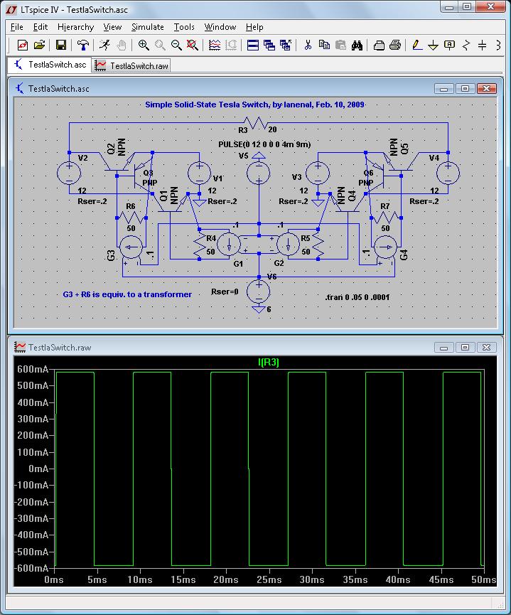
    I am copying also the .asc model file for my latest transformer version.
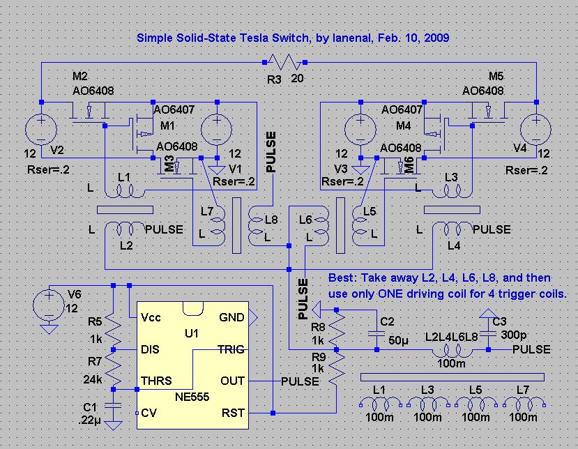
    I've just discovered your Simplest Solid State
    TS (transformer) circuit diagram.

    [Screenshot attached as thumbnail]

    Just this afternoon I was 'doodling' with paper
    and pencil and came up with a strikingly similar
    version! Questions have come up on the
    'other thread' regarding a solid state implementation
    so we've been collectively working towards a
    solution.

    With some time to kill I decided to peruse the
    forum Index in order to see if there were any other
    topics of interest and stumbled into your thread
    here.

    We agree on the number of MosFets and the
    manner in which they must be driven as
    'floating' switches. I notice however, that
    you've used a mix of P-channel and N-channel
    to manage the switching scheme. I've used
    all N-channel in my version.

    I notice you're using transformer coupling to
    drive the MosFet gates. Do you plan on
    driving the gates with a single pulse signal
    rather than 'complementary' signals devoted
    to the two separate 'groups' of MosFets?

    I'm unclear on interpreting the construct of
    your driver transformer, or transformers.
    Are you using several transformers or are
    you using a single transformer with multiple
    secondary windings? It appears that it is
    a single transformer...

    What provision do you plan to incorporate for
    're-setting' the core magnetism between
    drive pulses? Possibly C2 is the means?

    Your output line contains the two series
    capacitors C4 and C5 (100 uF each) which
    apply alternating current to the load.
    What is the intended purpose of the
    capacitors?


    Have you yet constructed the circuit to
    evaluate its operation?

    By the way, congratulations on arriving at
    the simplest circuit configuration! It's a
    great mental exercise.
    Last edited by SeaMonkey; 11-05-2010, 10:56 PM.

    Leave a comment:


  • Aromaz
    replied
    About Patent rights

    A short essay about patents and their rights. Something few people know or understand.

    In each and every country in the world where there is a form of patent rights there is also a time restriction for those patents to be valid. In the case of USA. UK, Canada, Australia, New Zealand, Isreal, Taiwan and South Africa; all underwriting the same patent applications:

    In these countries a patent is issed for a period not exceeding 20 years; from the date granted. Even so, there is an initial fee and an periodical fee to maintain such patent. On some items like medicine, the maximum period is often 5 years.

    If the periodical maintenance fee (usually every 3 years) are not paid, such patent rights are void from that due date. Further; it is for the owner of the patent to police his rights at his own cost; nobody else can, will or are alowed to do so.

    An application for 'International patent" is just that. It allows the applicant some form of protection while his application is under consideration. BUT - he still need to file applications IN EVERY COUNTRY seprately - within 6 months after issue in original country.

    Thus an patent issued in the USA but not completed in other countries are not valid in any such country. So if I apply for a patent in USA, it is granted and I then apply for the same in say 20 other counties whom all should approve; then there are still 170+ countries where my patent is non existing; and anybody in such country can in fact copy, produce and make money out of my patent.

    A calsical case in our realms is that of John Bedini - with USA patent and only international applications which was valid for 6 months......Thus JLN labs had no restrictions in France to copy, produce, sell any of his work.

    Then there are countries like most of South East Asia that requires for any patent holder to actually manufacture their product within the country within 6 months of granting the patent, else such patent is void.

    Again here is a good example: Microsoft does not need to produce their packages in more than only USA - it is easy to mass produce and ship anywhere in the world. Yet they have more than 72 production facilities worldwide. Until 2002 MS products were freely copied in Asia; not much could be done; but since they are now actually registering copyrights AND producing the produce in each of these countries, it is more difficult to get illegal copies; and police are getting much more income!

    So in short:
    To protect your design, you will in effect have to apply for patent in each and every one of 196 countries world wide; and you will have to comply with the restrictions in each of those countries - i.e. local production.

    In fact; very few (as in estimated 3%) of all USA patents are registered in more than 10 countries! None in 196 countries! Further, less than 37% of all USA patents are maintained longer than 12 years.

    As for Bell and Transistor; I doubt that they were in fact granted a patent. If there was something similar, it would be dated before 1950 - therefore long time expired. One of the conditions for a patent is that is has to be original: Bell Labs was not the original idea of the transistor - actually the transistor dates back to a patent issued to J.E. Lilienfeld in 1925 from Canada. Because that patent was only Canadian, and it anyway expired before 1945 .........

    One last thing: Patents are only issued to the actual human beings involved in the original design. Never to a company. Such person can assign the patent to their company/employer - but they remain the patent holder. When they die, their patent rights also die; and even the assignee can not enforce the patent.

    Leave a comment:


  • lanenal
    replied
    Rectified: I will build one when I get the skill, time and resource. Probably will also try other simpler projects to get more experiences first. As for the transistor, I just remember I read somewhere recently, and I googled it, but no luck of finding it again. Anyway, here is the link to the scientist I refered to: Lilienfeld. You can also find something about that in wikipedia.

    Leave a comment:


  • Rectified
    replied
    Xenomorph
    The statement made by Lanenal himself #25
    As for the title, it is meant to attract eyeballs. You won't know exactly what I will say until you actually read the whole post. So please don't judge by the title alone."Simply be able to do so with the circuit posted under that title? Or would he think he never will be able to understand this stuff, if this is what others call Simple? I would also advise my grandson if he were to put a circuit on the Internet called Simple

    Leave a comment:


  • lanenal
    replied
    Hi Rectified:

    Why not think in a more positive light? Since everybody is limited in one way or another, but everybody also has some unique gift, so how about some cooperation through the Internet, some kind of adventure that everybody participates, and once we reach the destination, what we found is unselfishly shared with all human kind? Would not that be thrilling?

    BTW, one small thing: transistors are usually mistaken to be invented by the Bell labs in 1940's, but way back in 1920's, a Canadian scientist already patented it. For that reason, the patent by Bell labs was later revoked.

    Leave a comment:


  • Xenomorph
    replied
    when a title or claims are made intentionally to draw others in
    The claim you made for your circuit, all though well intended, will be less offensive to some, once you perfect the circuit you propose
    WHERE HAS LANENAL EVER MADE ANY CLAIMS PEOPLE ???

    Point out the specific post please ! Do not project something that is not there.
    He has only stated that he works on the simulation of a simplified Tesla switch, not more not less.
    Compared to previous Tesla switch circuits (Bedini/Brand) this is indeed simpler.

    And i agree realizing this in the real world takes a lot of try and error. But if someone has nothing better to do, then why not.
    Last edited by Xenomorph; 02-14-2009, 11:04 PM.

    Leave a comment:


  • Rectified
    replied

    Leave a comment:


  • Xenomorph
    replied
    Nice one.
    Hehe i have been silly, i ran the simulation for a while with a battery voltage of 10 V to see if LTspice can simulate a cold charge, but "surprisingly" the battery voltage stayed constant. Maybe in version 5

    Leave a comment:


  • lanenal
    replied
    Thanks for pointing that out, Xenomorph. It turns out that can be replaced by 'u'.
    I corrected that in my post already, should have no problem anymore.
    In that version I also added a few labels to points of interest for measuring voltages.

    Originally posted by Xenomorph View Post
    @Lanenal: Thanks!

    For anyone who wants to try this and cant get it to work.
    The micro-character got lost in the ASCII copy-paste process.


    You have to replace the with the micro-character in LTspice.
    That is for all capacitors in the microfarad range.
    Last edited by lanenal; 02-14-2009, 05:04 PM.

    Leave a comment:


  • Xenomorph
    replied
    @Lanenal: Thanks!

    For anyone who wants to try this and cant get it to work.
    The micro-character got lost in the ASCII copy-paste process.

    SYMATTR InstName C1
    SYMATTR Value .1?
    You have to replace the
    ?
    with the micro-character in LTspice.
    That is for all capacitors in the microfarad range.

    Leave a comment:


  • lanenal
    replied
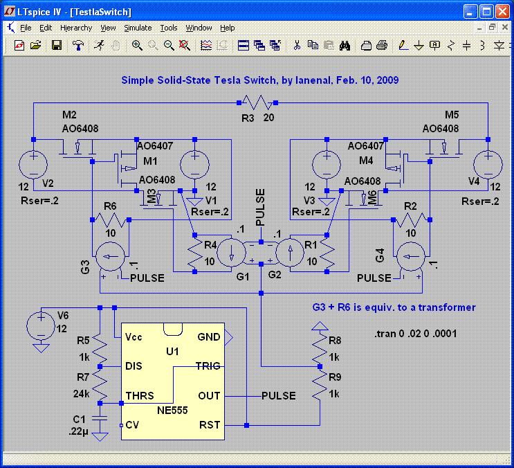
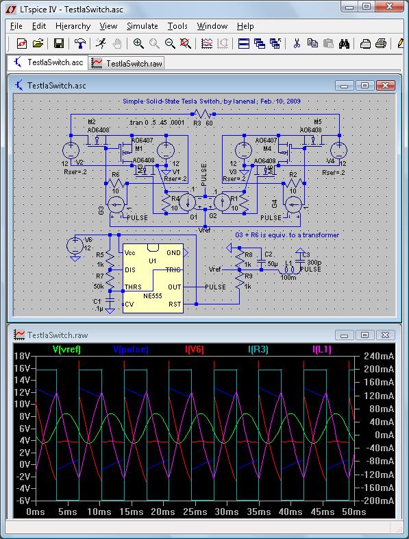
    simulation with transformer

    I am copying also the .asc model file for my latest transformer version. Just copy and past into a text editor and save as "TeslaSwitch.asc". Hopefully this will work. My simulation result is attached. You can get LTspice free.

    Version 4
    SHEET 1 1188 824
    WIRE 304 -64 -16 -64
    WIRE 704 -64 384 -64
    WIRE 16 0 16 -32
    WIRE 16 0 -16 0
    WIRE 112 0 112 -32
    WIRE 176 0 112 0
    WIRE 304 0 176 0
    WIRE 512 0 384 0
    WIRE 576 0 576 -32
    WIRE 576 0 512 0
    WIRE 672 0 672 -32
    WIRE 704 0 672 0
    WIRE -16 16 -16 0
    WIRE 16 16 16 0
    WIRE 128 16 96 16
    WIRE 176 16 176 0
    WIRE 304 16 304 0
    WIRE 384 16 384 0
    WIRE 512 16 512 0
    WIRE 592 16 560 16
    WIRE 672 16 672 0
    WIRE 704 16 704 0
    WIRE 128 32 128 16
    WIRE 560 32 560 16
    WIRE 128 48 128 32
    WIRE 560 48 560 32
    WIRE 112 96 112 0
    WIRE 112 96 96 96
    WIRE 576 96 576 0
    WIRE 592 96 576 96
    WIRE -16 112 -16 96
    WIRE 176 112 -16 112
    WIRE 272 112 272 80
    WIRE 304 112 304 96
    WIRE 304 112 272 112
    WIRE 384 112 384 96
    WIRE 416 112 416 80
    WIRE 416 112 384 112
    WIRE 704 112 704 96
    WIRE 704 112 512 112
    WIRE 304 128 304 112
    WIRE 384 128 384 112
    WIRE 208 160 192 80
    WIRE 256 160 208 160
    WIRE 272 160 256 160
    WIRE 432 160 416 160
    WIRE 480 160 496 80
    WIRE 480 160 432 160
    WIRE 48 176 16 176
    WIRE 336 176 48 176
    WIRE 384 176 336 176
    WIRE 16 224 16 176
    WIRE 480 224 480 192
    WIRE 560 224 480 224
    WIRE 48 240 48 176
    WIRE 64 240 48 240
    WIRE 560 240 560 224
    WIRE 672 240 672 192
    WIRE 64 304 16 304
    WIRE 288 304 176 304
    WIRE 480 304 416 304
    WIRE 560 304 480 304
    WIRE 592 304 560 304
    WIRE 704 304 672 304
    WIRE 368 368 288 368
    WIRE 64 384 64 368
    WIRE 64 384 16 384
    WIRE 176 384 176 304
    WIRE 176 384 64 384
    WIRE 336 432 336 176
    WIRE 336 432 288 432
    WIRE 480 432 480 384
    WIRE 480 432 336 432
    FLAG 304 128 0
    FLAG 384 256 0
    FLAG 16 448 0
    FLAG 288 240 0
    FLAG 480 192 0
    FLAG 368 368 TP
    FLAG 704 304 TP
    FLAG 672 192 0
    FLAG 416 304 Vref
    FLAG 16 16 Left
    FLAG 384 128 0
    FLAG 672 16 Right
    FLAG 128 48 Glu
    FLAG 560 48 Gru
    FLAG 416 160 Grd
    FLAG 272 160 Gld
    SYMBOL voltage 304 0 R0
    WINDOW 123 0 0 Left 0
    WINDOW 39 -94 14 Left 0
    WINDOW 0 -30 -15 Left 0
    WINDOW 3 2 7 Left 0
    SYMATTR SpiceLine Rser=.2
    SYMATTR InstName V1
    SYMATTR Value 12
    SYMBOL voltage -16 0 R0
    WINDOW 123 0 0 Left 0
    WINDOW 39 -33 132 Left 0
    WINDOW 0 -33 102 Left 0
    WINDOW 3 3 101 Left 0
    SYMATTR SpiceLine Rser=.2
    SYMATTR InstName V2
    SYMATTR Value 12
    SYMBOL voltage 384 160 R0
    WINDOW 123 0 0 Left 0
    WINDOW 39 -7 -5 Left 0
    WINDOW 0 37 34 Left 0
    WINDOW 3 34 62 Left 0
    SYMATTR InstName V6
    SYMATTR Value 12
    SYMBOL pmos 128 112 M180
    WINDOW 0 23 158 Left 0
    WINDOW 3 2 130 Left 0
    SYMATTR InstName M1
    SYMATTR Value AO6407
    SYMBOL nmos 16 16 R270
    WINDOW 0 96 37 VRight 0
    WINDOW 3 67 19 VRight 0
    SYMATTR InstName M2
    SYMATTR Value AO6408
    SYMBOL nmos 176 160 R270
    WINDOW 0 3 -63 VRight 0
    WINDOW 3 26 -88 VRight 0
    SYMATTR InstName M3
    SYMATTR Value AO6408
    SYMBOL Misc\\NE555 176 336 M0
    SYMATTR InstName U1
    SYMBOL res 32 208 M0
    SYMATTR InstName R5
    SYMATTR Value 1k
    SYMBOL res 32 288 M0
    SYMATTR InstName R7
    SYMATTR Value 50k
    SYMBOL cap 32 384 M0
    WINDOW 0 46 36 Left 0
    WINDOW 3 40 62 Left 0
    SYMATTR InstName C1
    SYMATTR Value .1u
    SYMBOL res 464 208 R0
    SYMATTR InstName R8
    SYMATTR Value 1k
    SYMBOL res 464 288 R0
    SYMATTR InstName R9
    SYMATTR Value 1k
    SYMBOL ind2 688 288 R90
    WINDOW 0 5 56 VBottom 0
    WINDOW 3 32 56 VTop 0
    SYMATTR InstName L1
    SYMATTR Value {G}
    SYMATTR SpiceLine Rser=4
    SYMATTR Type ind
    SYMBOL cap 544 240 R0
    WINDOW 0 37 30 Left 0
    WINDOW 3 24 -3 Left 0
    SYMATTR InstName C2
    SYMATTR Value 500u
    SYMBOL cap 656 240 R0
    WINDOW 3 22 -25 Left 0
    SYMATTR Value 900p
    SYMATTR InstName C3
    SYMBOL cap -32 -64 R0
    WINDOW 0 21 14 Left 0
    WINDOW 3 5 -19 Left 0
    SYMATTR InstName C5
    SYMATTR Value 100u
    SYMATTR SpiceLine Rser=0.1
    SYMBOL ind 400 -80 R90
    WINDOW 0 5 56 VBottom 0
    WINDOW 3 32 56 VTop 0
    SYMATTR InstName Load
    SYMATTR Value 100m
    SYMATTR SpiceLine Rser=9
    SYMBOL ind2 176 96 R270
    WINDOW 0 33 34 VTop 0
    WINDOW 3 63 75 VBottom 0
    SYMATTR InstName L2
    SYMATTR Value {G}
    SYMATTR Type ind
    SYMBOL ind2 112 0 M0
    SYMATTR InstName L3
    SYMATTR Value {G}
    SYMATTR Type ind
    SYMATTR SpiceLine Rser=4 Cpar=5u
    SYMBOL voltage 384 0 M0
    WINDOW 123 0 0 Left 0
    WINDOW 39 -94 14 Left 0
    WINDOW 0 -30 -15 Left 0
    WINDOW 3 2 7 Left 0
    SYMATTR SpiceLine Rser=.2
    SYMATTR InstName V3
    SYMATTR Value 12
    SYMBOL voltage 704 0 M0
    WINDOW 123 0 0 Left 0
    WINDOW 39 -33 132 Left 0
    WINDOW 0 -33 102 Left 0
    WINDOW 3 3 101 Left 0
    SYMATTR SpiceLine Rser=.2
    SYMATTR InstName V4
    SYMATTR Value 12
    SYMBOL pmos 560 112 R180
    WINDOW 0 23 158 Left 0
    WINDOW 3 2 130 Left 0
    SYMATTR InstName M4
    SYMATTR Value AO6407
    SYMBOL nmos 672 16 M270
    WINDOW 0 96 37 VRight 0
    WINDOW 3 67 19 VRight 0
    SYMATTR InstName M5
    SYMATTR Value AO6408
    SYMBOL nmos 512 160 M270
    WINDOW 0 1 -73 VRight 0
    WINDOW 3 26 -88 VRight 0
    SYMATTR InstName M6
    SYMATTR Value AO6408
    SYMBOL cap 720 -64 M0
    WINDOW 0 21 14 Left 0
    WINDOW 3 5 -19 Left 0
    SYMATTR InstName C4
    SYMATTR Value 100u
    SYMATTR SpiceLine Rser=0.1
    SYMBOL ind2 400 96 R270
    WINDOW 0 33 34 VTop 0
    WINDOW 3 63 75 VBottom 0
    SYMATTR InstName L4
    SYMATTR Value {G}
    SYMATTR Type ind
    SYMBOL ind2 576 112 M180
    WINDOW 0 36 80 Left 0
    WINDOW 3 36 40 Left 0
    SYMATTR InstName L5
    SYMATTR Value {G}
    SYMATTR Type ind
    SYMATTR SpiceLine Rser=4 Cpar=5u
    TEXT 536 440 Left 0 !.tran 0 .1 0 .0001
    TEXT 32 480 Left 0 ;Simple Solid-State Tesla Switch, by lanenal, Feb. 10, 2009
    TEXT 560 368 Left 0 !.param G 50m
    TEXT 504 408 Left 0 !K1 L1 L2 L3 L4 L5 1
    Attached Files
    Last edited by lanenal; 02-14-2009, 04:59 PM. Reason: adding labels to the schema

    Leave a comment:


  • sucahyo
    replied
    Thanks for the explanation, I will learn how it work.

    Leave a comment:


  • lanenal
    replied
    @sucahyo

    I think you are right about 4 steps. but not sure what you mean by 'line'? I guess you mean substituting the MOSFETs by switches? Anyway, here are the description:

    The sequences are, as I understood it (but correct me if I got it wrong):

    1. the pulse voltage Vp is at zero, which is much lower than the reference voltage Vr: M1 open, M2 and M3 closed, so V1 and V2 are connected in parallel; M4 closed, M5 and M6 open, so V3 and V4 are connected in series.
    Result: the left end of the load is at 12V, and the right end of the load is at 24V.

    2. the pulse voltage Vp is at 6V (when it rises from zero to 12V, usually in nanoseconds), which is very close to the reference voltage Vr: M1 open, M2 and M3 open, so V1 and V2 are NOT connected; M4 open, M5 and M6 open, so V3 and V4 are NOT connected (NOTE: NOT connected can be read as having a very very high resistance, say in 1000 mega-ohms).
    Result: the left end of the load is going from 12V to 24V, and the right end of the load is dropping from 24V to 12V.

    3. the pulse voltage Vp is at 12V, which is much higher than the reference voltage Vr: M1 closed, M2 and M3 open, so V1 and V2 are connected in series; M4 open, M5 and M6 closed, so V3 and V4 are connected in parallel.
    Result: the left end of the load is at 24V, and the right end of the load is at 12V.

    4. the pulse voltage Vp is at 6V (when it falls from 12V to zero, usually in nanoseconds), which is very close to the reference voltage Vr: M1 open, M2 and M3 open, so V1 and V2 are NOT connected; M4 open, M5 and M6 open, so V3 and V4 are NOT connected (NOTE: NOT connected can be read as having a very very high resistance, say in 1000 mega-ohms).
    Result: the left end of the load is dropping from 24V to 12V, and the right end of the load is going from 12V to 24V.

    Then it repeats itself, going back to 1.


    Originally posted by sucahyo View Post
    No one ever build it with three battery?

    I don't know how to read the diagram.

    Question:
    @lanenal, can you replace the MOSFET with line? So, if there are 4 sequence then can you show 4 picture with different line?


    @all
    anyone ever made the battery switching different from battery pulsing? I am thinking to reduce batery ON time when all that we need is coil shut off spike.
    Last edited by lanenal; 02-13-2009, 05:35 PM.

    Leave a comment:


  • lanenal
    replied
    Xenomorph: Thanks for your encouragement! I am OK though, Joit is not completely negative, his emphasis on experiment is quite constructive.

    lanenal

    Originally posted by Xenomorph View Post
    Just keep on flaming here guys, that way we will never soon realize a solid state tesla switch effort.
    I still dont understand the amount of negative feelings towards lanenal.
    If he would be frustrated now and keep on working in his own without posting here it would be thanks to people like Joit depreciating his benevolent input.
    I can only encourage lanenal to continue sharing his findings without becoming a victim of psychopathic frustrative projections with no constructive intent.

    Leave a comment:


  • sucahyo
    replied
    Originally posted by citfta View Post
    For the tesla switch to do what it is supposed to do you have to connect two of the batteries in series and at the same time connect the other two in parallel. This means that the switches have to follow a certain sequence when they are energized.
    No one ever build it with three battery?

    I don't know how to read the diagram.

    Question:
    @lanenal, can you replace the MOSFET with line? So, if there are 4 sequence then can you show 4 picture with different line?


    @all
    anyone ever made the battery switching different from battery pulsing? I am thinking to reduce batery ON time when all that we need is coil shut off spike.
    Last edited by sucahyo; 02-13-2009, 08:43 AM.

    Leave a comment:

Working...
X